Professor / Dr. Afshin Rashid (PhD in Nano-Microelectronics) Faculty member in islamic azad university science and reserch branch tehran (electronic department) assistant professor 🏆 In 2023, he has won the title of "top two percent scientist in the world" from the perspective of Elsevier Publishing Institute.
Mr. Dr. Afshin Rashid, Born on , (1989 _ April 5) in Tehran , is a professor (Electrical Department - Micro and Nano Electronic Devices) and a member of the scientific faculty of Islamic Azad University, Tehran Science and Research Branch; They have 21 conference papers inside the country and 100 international ISI papers abroad. His published articles are mostly on specialized topics of nanoelectronics, nanotransistors, electric nanochips, electronic nanowires, and micro and nanoelectronic devices. have acquired Elsevier publications. There are many books, articles and conferences focusing on nanoelectronics technology from him, and he is an amazing invention in the field of nanotechnology, as well as (the most indicative theory of internal system change and redesign of CDSE electronic nanosensors).🏆 In 2023, he has won the title of "top two percent scientist in the world" from the perspective of Elsevier Publishing Institute.
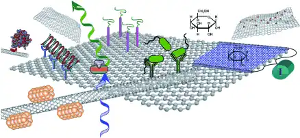
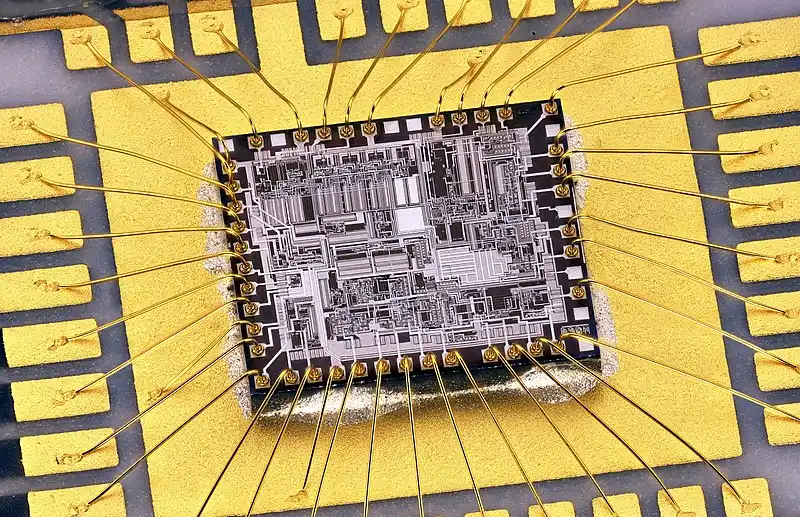
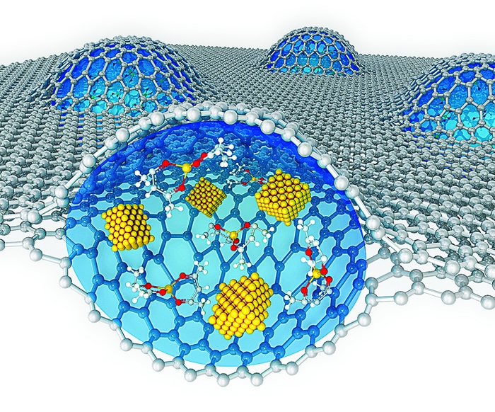
Nano-biosensors and nano-biochips in moving nano-particle molecules through dielectric enhancement through vertical nano-gap architectures
We Respect The Science
|
Jan 5 ,
2024
Note: The dynamic process of sorting and precise positioning of nanoparticle biomass in pre-defined microstructures is very important, however, this is a major obstacle to the realization of surface-sensitive nanobiosensors and practical nanobiochips.
A scalable, widespread and non-destructive trapping method based on dielectric forces is much needed for nanoparticle collection and nanobiosensing tools. Here, we present a vertical nanogap architecture with an electrode-insulator-electrode stack structure. Facilitate the generation of strong dielectric forces at low voltages, for precise capture and manipulation of nanoparticles and molecular assemblies, including lipid vesicles and amyloid-beta fibrillar proteins/oligomers. Our vertical nanoplastic platform allows low-voltage nanoparticles recorded in optical dimensional designs, providing new opportunities for the fabrication of advanced surface-sensitive sensors.
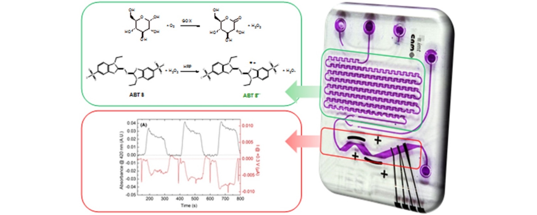
Nano biosensors appear as a powerful alternative to conventional analytical techniques, as nanosensors perform highly sensitive, real-time, and high-frequency monitoring of pollutants without extensive sample preparation. Nano biosensors can be integrated into small devices for rapid screening and monitoring of a wide range of pollutants. Since the nano biosensor is an analytical device, used to detect a chemical substance, which is a combination of a biological component with a physicochemical detector. A sensitive biological element , eg tissue, micro-organisms , etc., a component of a material or biomimetic that interacts with and binds to nanoparticles.
A biosensor typically consists of a bioreceptor (enzyme/antibody/cell/nucleic acid/aptamer), a transducer component (semiconductor material/nanomaterial) and an electronic system that includes a signal amplifier , processor and screen. It is a show. Transducers and electronics can be combined, for example, in CMOS-based microsensor systems . The detection component, often called a biological receptor, uses biomolecules from living organisms or organisms modeled after biological systems to interact with the analyte of interest. This interaction is measured by the transmitter transmitter, which gives a measurable signal proportional to the presence of the target analyte in the sample.
Conclusion :
In , the dynamic process of sorting and accurate positioning of nanoparticle biomasses in predefined microstructures is very important, however, this is a major obstacle to the realization of surface-sensitive nanobiosensors and practical nanobiochips.
Molecular Nanoelectronics and Graphene Molecular Nanomemories A Novel non-volatile Charge Trapping Memory Using isolated and uniformly distributed graphene nanocrystals as a nano floating gate
We Respect The Science
|
Jan 4 ,
2024
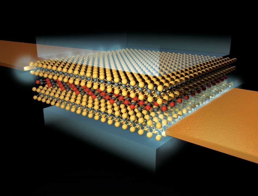
Note: Graphene molecular nano memories are a new non-volatile charge trapping memory using isolated and uniformly distributed graphene nano crystals as a nano floating gate with controllable capacity and excellent uniformity. The nanographene charge-trapping memory exhibits large gate memory (4.5 V) at low operating voltage (8 V), chemical and thermal stability (1000 °C), as well as tunable memory performance using differential tunneling. .
Graphene has outstanding nanoelectronic properties, very high electron mobility and unparalleled conductivity at the nanoscale. It is a super conductor that transfers electrons ten times faster than silicon. These characteristics have made graphene an ideal candidate for next-generation nanoelectronic applications such as graphene molecular nano-memories .
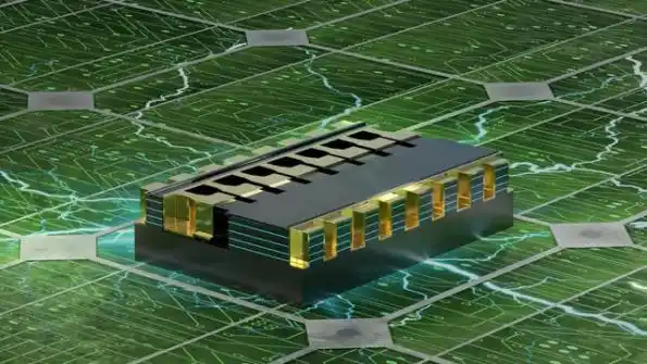
The interaction of the electronic particles of the adsorbed nano-graphene, which causes a change in the electrical conductivity on the surface of the molecular nano-memories of nano-memory molecular graphene . The absorption of a small amount of nano-electrons with a very low molecular movement changes the resistance of nano-graphene , which corresponds to Nano Memory Moulcolar . Nano Memory Moulcolar is a transparent flexible nanographene floating gate transistor nano memory device that is made by combining a single-layer graphene active channel with gold nanoparticle charge trap elements. Systematically, the sizes of gold nanoparticle charge trap elements, the thickness of the tunneling dielectric layer and the doping level of graphene are very important in its production. In particular, the conductance differences ( ie , memory window) between program and erase operations at a given read gate voltage can be maximized through doping. The resulting molecularly developed graphene nano-memories provide excellent programmable nano-scale memory performance compared to previous graphene memory devices and a large memory window (12 V), fast switching speed (1 μs), capability It shows strong electrical reliability. Graphene molecular nanomemories show unique electronic properties, and its small dimensions, structural strength, and high performance make it very promising as a charge storage medium for nanomemory applications. Along with the development of miniaturized and enlarged devices, nanostructured graphene appears as an ideal material.
Testing the link between Nano Memory Moulcolar Graphene Molecular Nano Memories and Graphene Nano Transistors to Reproduce and Produce This Type of Electrical Nano Memory.
We Respect The Science
|
Jan 17 ,
2024
Note: Graphene, which consists of only one carbon atom, can be used to create multi-layer graphene molecular nano memories that consume less energy and occupy little space. Graphene is a semi-conducting material with zero gap and not suitable for logic circuits, but using nano technology, they create different forms of this material that have different gaps.
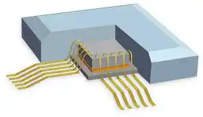
Graphene nanoribbons, multilayer graphene and graphene grown on Si are such forms. The term "nano-transistor" comes from the combination of the word "nano-scale" in transmission and resistance. In a Si graphene field effect nano transistor, the resistance between two electrodes can be transferred or controlled by a third electrode. In a Si multilayer graphene field effect nano transistor, the current between the two electrodes is controlled by the electric field from the third electrode. Unlike the bipolar transistor, it is capacitively connected to the third electrode and is not in contact with the semiconductor. Three electrodes are connected to the source, drain and gate in the structure and internal structure of multilayer graphene molecular nano memories .
By using the structure of nanomolecular memory , the size of the memory bits can be basically reduced, thereby increasing the density of the magnetic memory and its efficiency, and lowering its cost. Nano lithography methods are now being used to prepare some very powerful memories. The science and technology of nanoelectronics provide different possibilities of nano molecular memory . For example, photorefractory materials represent only one type of optical memory. In fact, by using nano technology, the storage capacity of information can be increased by a thousand times or more. Storing subject information is very important and necessary, which can be done in different ways through nanomolecular memories .The role of graphene nanosheets (GA) in the construction of nanotransistor (Nano Transistor) in the form of an electric field created by the gate electrode controls the current created by the source and drain electrodes. Drain current transport is modulated by changing the density of charge carriers in the two-dimensional transport channel. In the multilayer Si graphene field effect nanotransistor, a 3D transmission channel, the drain current is modulated by the thickness of the 3D transmission channel. In the circuit diagram of a multilayer GA graphene field effect nanotransistor, the source and drain electrodes are directly connected to the semiconductor. While the gate electrode is capacitively connected to the semiconductor using gate dielectric. Many chemical and physical methods have been proposed to produce different types of multilayered nanographene.
Experiment (nanoelectronic memory) using small chlorophyll-like organic molecules instead of charge storage capacitors
We Respect The Science
|
Jan 18 ,
2024
Note: In electrical conduction from a conductor to a semiconductor or an insulator, nanotubes can be electrically changed depending on their structure and molecular chiral angle . Since carbon nanotubes are able to pass electric current through their surface by means of ballistic transfer of electrons without friction - this current is a hundred times higher than the current that passes through copper wire - so nanotubes are an ideal choice for making nano chips . memory clouds are memory clouds .
Making nano memory cloud chips Nano memory cloud is made of carbon nanotubes , although the discovery of small but very resistant, flexible and conductive carbon nanotubes with dimensions equal to DNA strands and the use of tiny organic molecules Chlorophyll instead of charge storage capacitors in nano-type memory chips. Nano crystals, the use of which will increase the lifespan of nano memories.
In fact, by using nano technology, the storage capacity of information can be increased by a thousand times or more. The storage of subject information is very important and necessary, which can be done in different ways through nano cloud memories . One of the new information storage tools is the use of nickel quantum dots in nanometer sizes, which are expected to be used to store terabytes of data. According to the cloud of nano memories, there is a high potential for activity in this field. The structure and structure of supercapacitors based on nanoelectronics store 100 times more charge than electrolyte types in the same volume and charge and discharge at a much faster rate than batteries.
Of course, these capacitors still store up to 10 times less charge than some types of batteries in the same volume. According to these characteristics, supercapacitors are used in cases where frequent charging and discharging are required, high charging speed is required, or sudden discharge of the charge is required. (Until now, their main use in the electronics industry has been as a backup for SRAM memories.) Nanoelectronics shows a schematic of a supercapacitor. The main idea to achieve high capacitance is to reduce the distance between positive and negative charges in the capacitor. The design of these capacitors is such that the thickness of the dielectric layer in them does not exceed one or more molecules.
Science and technology of nanoelectronics and testing the possibilities of nano memories (Nano molecular memory)
We Respect The Science
|
Jan 2 ,
2024
Note: Common nanoelectronics technologies in nanomemories hardly meet the demands, but nanotechnology offers better solutions. One of the new means of data storage is the use of nickel quantum dots in nanometer sizes, which are expected to be used to store terabytes of data, even in homes and in personal use.
Given the relatively large (physically speaking) storage devices we have now and the fact that we need gigabyte sizes in various areas, there is a huge potential for activity in this area.Each quantum dot consists of a single ball of several hundred atoms that can have one of two magnetic states. This allows them to contain a single bit of information (zero or one), as is customary in machine computing. In conventional hard disks, the data bits must be spaced far enough apart to avoid reciprocation. Quantum dots act as completely independent units that are not structurally connected, so they can become somewhat closer to each other. They can be arranged to a certain density that allows any type of information to be stored up to 5 terabytes in a space the size of a postage stamp. Activities should continue until these nanodots work better and work with other computing devices such as silicon chips.
By using the structure of nanomolecular memory , the size of the memory bits can be basically reduced, thereby increasing the density of the magnetic memory and its efficiency, and lowering its cost. Nano lithography methods are now being used to prepare some very powerful memories. The science and technology of nanoelectronics provide different possibilities of nano molecular memory . For example, photorefractory materials represent only one type of optical memory. In fact, by using nano technology, the storage capacity of information can be increased by a thousand times or more. Storing subject information is very important and necessary, which can be done in different ways through nanomolecular memories .One of the new information storage tools is the use of nickel quantum dots in nanometer sizes, which are expected to be used to store terabytes of data. According to nano molecular memories, there is a high potential for activity in this field.
The Use of Quantum Dots in The Production Of Nanosensors
We Respect The Science
|
Jan 17 ,
2024
Quantum dots are defined as small semiconductor crystals. By controlling the dimensions of the quantum dots, the electromagnetic field emits light in different colors and wavelengths. For example, quantum dots made of cadmium arsenide with dimensions of 3 nm emit green light; While particles with a size of 5.5 nanometers of the same material emit red light. Due to the ability to produce light at specific wavelengths of quantum dots, these tiny crystals are used in optical devices. In this field, quantum dots can be used in making infrared detectors, light emitting diodes . Infrared detectors are extremely important. The main problem of these detectors is their cooling . Liquid oxygen and electronic cooling are used to cool these detectors. These detectors must work at very low temperatures, close to 31 degrees Kelvin, to function properly, so they cannot be used at room temperature, while detectors made using quantum dots can be easily used at room temperature.
The use of nanotubes in the production of nanosensors
Due to their unique mechanical and electronic properties, single-walled and multi-walled carbon nanotubes have found various applications, including their use as sensors with very high accuracy to detect substances at very low concentrations and at high speeds. did
In general, the use of nanotubes in sensors can be divided into two categories:
A ) Carbon nanotubes as chemical sensors: These sensors can detect very small concentrations of gas molecules with very high sensitivity at room temperature. Chemical sensors include collections of single-walled nanotubes and can detect chemicals such as nitrogen dioxide and The electrical conductivity of a single-walled semiconductor nanotube placed in the vicinity of 0.11 ppm of nitrogen dioxide can be tripled within seconds, and the conductivity will double for adding just 0% ammonia. Sensors made of single-walled nanotubes have high sensitivity and quick response at room temperature.These properties have important results in diagnostic applications.
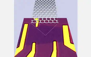
Scanning Tunneling Microscope (STM) or Scanning Probe Nano Lithography or (SPL) in the Range (Below 20 Nanometers)
Elsevier Bv
|
Jan 18 ,
2024
The use of AFM for scanning probe lithography also suffers from power-related problems, but it is better suited than STM for this task due to the less stringent requirements of the technique: no very high vacuum conditions. , conductive surface or very good tip-to-sample distance control is required. Scanning probe nanolithography based on AFM can be performed through different mechanisms and offers a wide range of possibilities . Therefore, the AFM tip can produce localized changes in the composition, height, or physical/chemical properties of surfaces through thermal effects, mechanical effects, deposition, chemical effects, etc. The principle of this technique for making electronic nano devices has been drawn and the example of making Si nanowires based on the oxidation of nanolithography probe Scanning is done. A derived technique that has become very popular is dip-pen nanolithography, in which the tip deposits specific inks with excellent clarity at desired locations.
Fabrication of "bio-electronic nano-sensors" using the theory of activation of metal nano-tube hybridization
afshin rashid
|
Jan 4 ,
2023
Note: There are several problems with the methods of making bioelectronic nanosensors using metal nanotube hybridization functionalization . First of all, most of the nanotubes are functionalized and as a result the electronic structure of SWCNTs is defective. Second, due to the strong reaction, it is difficult to purify the product from amorphous carbon. The most important thing is that there is no covalent reaction after which the (m,n) nanotube can be uniquely purified.
Testing Nano Memories Based On a Particle Enclosed in a (One-Dimensional Nano Memory)
We Respect The Science
|
Jan 26 ,
2023
Note: Nanotechnology is used in quantum computing and other similar electronic technologies. There are two basic principles at the core of nanotechnology: First, the smaller you make the material, the larger the relative surface area of the material. And the second is the loss of bulk properties instead of quantum phenomena when you get to such a small scale.
Quantum nanotechnology is based on the principle of electron tunneling. The basic theory is that a particle trapped in a one-dimensional nanomemory cannot escape unless an electron breaks its way out of the confinement. This is a phenomenon that is only exhibited by quantum materials and cannot be seen with any bulk material. This principle can be extended to include all 3D - the so-called particle in a 3D nano-memory. The amount of electron confinement introduced into a material determines its dimension - because quantum dimensions are more relative to electron confinement (and in how many dimensions electrons operate in) than atomic spatial arrangement. Quantum dots are probably the most well-known quantum structure in nano-memories. The interesting thing about quantum dots is that electronically, they are confined in all three dimensions, so they are classified as zero-dimensional materials.


 Professional Skills
 Research Experience
 Work Experience
 Education

 Judge of The Works of Others
 Patents
 Media Publications


 Prizes and Awards